
The Weight of 'Packaging' Symbolized by the Chairman’s On-Site Visit

On November 1, 2026, Samsung Electronics Chairman Lee Jae-yong visited Samsung Electronics’ 'Advanced Packaging Lab (APL)' in Yokohama, Japan, to directly inspect the status of future semiconductor packaging technologies 12. This on-site visit is interpreted as a significant management move aimed at directly verifying the status of packaging technology, which has emerged as a key competitive strength in the semiconductor industry, and to finalize the direction of the future technology roadmap 1.
The reason advanced packaging is so important is that it offers an alternative to ultra-fine process technologies that have reached their physical limits. Advanced packaging is a back-end process technology that integrates individual semiconductors, such as artificial intelligence (AI) accelerators and high-bandwidth memory (HBM), into a single unit 3. At a time when ultra-fine process technologies are facing physical limits, packaging technology has emerged as a core factor determining the final performance of AI semiconductors 3. Considering this technical importance, the Chairman’s visit demonstrates how aggressively Samsung Electronics is driving efforts to gain an advantage in advanced packaging technology amidst the restructuring of the global semiconductor supply chain and the advent of the AI era 1.
Yokohama APL: A Laboratory for Cooperation in Materials, Parts, and Equipment
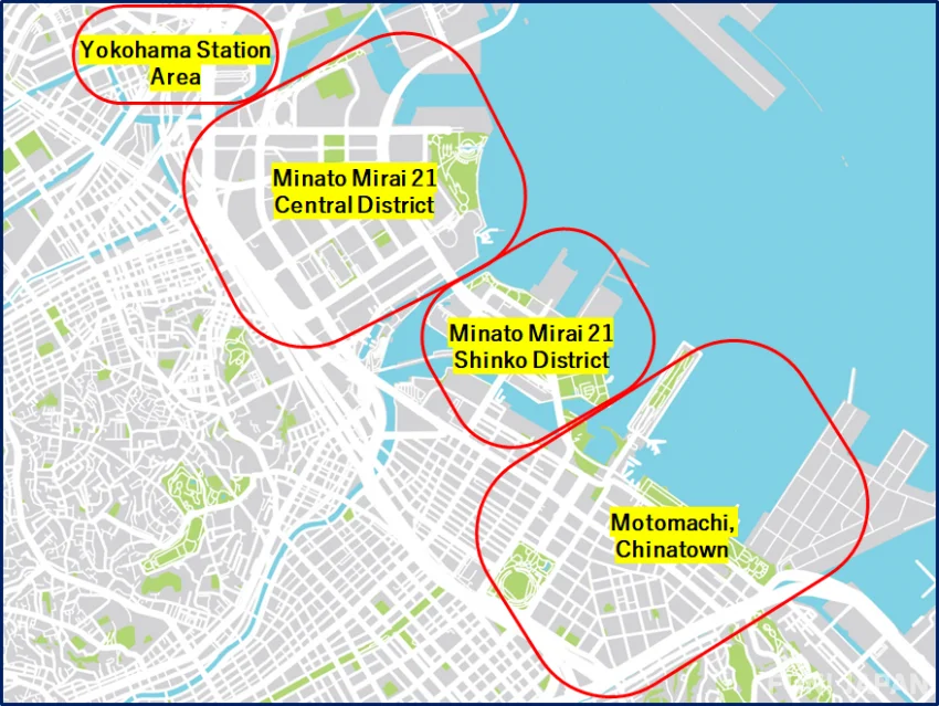
Samsung Electronics’ APL held its opening ceremony on September 8, 2026, in Minatomirai, Yokohama 34. This research lab serves not merely as a production base but plays a core role in developing next-generation packaging technologies through cooperation with local materials, parts, and equipment companies and research institutions 34. Samsung Electronics plans to invest approximately 40 billion yen (roughly 350 billion to 360 billion won) in the APL over five years starting in 2024 34.
The background for choosing Yokohama as a research hub lies in the robust ecosystem the region possesses. The Yokohama area is advantageous for securing research talent due to the concentration of prestigious universities such as the University of Tokyo and Yokohama National University 3. Additionally, the presence of world-class semiconductor materials, parts, and equipment companies like Resonac and Disco provides an optimal location for technological development and cooperation 3. Samsung Electronics’ strategy is to consolidate its technological superiority by combining this Japanese materials, parts, and equipment ecosystem with its own semiconductor design and manufacturing capabilities 3.
Securing Talent and Building a Korea-Japan Cooperation Network
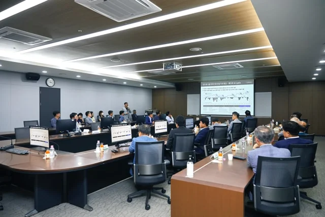
Ultimately, 'people' are necessary for technological development. Samsung Electronics has established a plan to secure more than 100 local semiconductor specialists at the APL by 2027 34. This is analyzed as an intention to accelerate the development of next-generation packaging technologies by leveraging local excellent research talent 3.
Speed has also increased in building a cooperation network since the opening. Immediately after the APL opened, Chairman Lee Jae-yong held a lunch meeting in Seoul on September 14, 2026, with a visiting Japanese House of Councillors delegation 56. Daisaku Hiraki, a member of the House of Councillors, attended the meeting, and they discussed semiconductor industry prospects in the AI era and areas of Korea-Japan cooperation 56. These moves are on the extension of the May 2023 Korea-Japan summit, which sought to develop cooperative relations for strengthening the semiconductor supply chain beyond past conflicts between the two countries 4.
Honam vs. Japan: Views on Investment Destinations
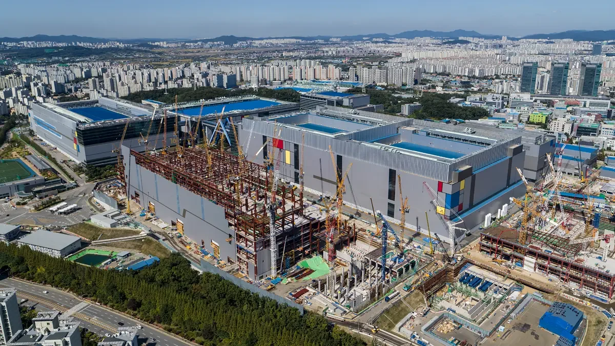
Some are watching to see how Samsung Electronics’ R&D moves toward Japan will balance with domestic semiconductor projects. While Samsung Electronics is building a large-scale R&D hub in Yokohama, issues regarding infrastructure construction related to the domestic Honam region semiconductor megaproject have been raised 56. In the case of the Honam semiconductor megaproject, the power supply agreement signed by KEPCO, the Ministry of Climate, Energy and Environment, Gwangju City, Samsung Electronics, and SK Hynix is planned to be fulfilled as scheduled 56.
However, semiconductor industry analysts argue that the ability to secure necessary infrastructure and talent in both countries, along with the associated costs and timelines, will be a key factor determining the execution speed of each investment plan 56. Although Samsung Electronics has not withdrawn from participating in the domestic Honam project, Japan’s stable power supply environment and formation of a materials, parts, and equipment cluster remain quite attractive from an R&D perspective.
Synergy Between AI Ecosystem Expansion and Packaging Technology

This technological inspection aligns with Samsung Electronics’ company-wide AI transformation (AX) strategy. Linked to the inspection of semiconductor packaging technology, Samsung Electronics has recently been accelerating the construction of an AI semiconductor ecosystem 1. For example, on October 31, 2026, it held an 'AI Innovation' briefing with Sam Altman, CEO of OpenAI, strengthening its 'AI Driven' management 12.
The goal is to secure comprehensive technological leadership encompassing both hardware, such as semiconductor packaging technology, and software, such as the AI ecosystem 1. Especially with the rapid growth of the AI semiconductor market, competition among global companies in packaging technology is intensifying day by day. The combination of hardware and software signifies platform-level competitiveness beyond simple performance improvements 31.
Conclusion: A New Form of Alliance Toward 'Technological Sovereignty'

Ultimately, this on-site visit and the role of the APL demonstrate a form of 'pragmatic technological alliance' that goes beyond past trade conflicts. Combining Japan’s strong ecosystem in materials, parts, and equipment with Korea’s manufacturing and design capabilities is a rational choice to secure an advantage in back-end technology competition, which is essential in the AI semiconductor era 23.
Through securing more than 100 local talents by 2027 and cooperation with the Japanese government, local governments, and materials, parts, and equipment companies, Samsung Electronics is laying the foundation to take the lead in next-generation 3D packaging technology 43. This move clearly indicates how important it is for companies to build technology cooperation networks that break down borders and ecosystems as the global semiconductor supply chain becomes increasingly complex due to geopolitical issues 4.
References
- 이재용 삼성전자 회장, 미래 반도체 패키징 기술 일본 현장 점검 – 삼성전자 뉴스룸 · news.samsung.com↩
- 이재용, 일본 요코하마 반도체 패키징 연구거점 점검 … AI 반도체 기술 주도권 확보 나서 · worktoday.co.kr↩
- 삼성전자, 요코하마에 첨단패키징 연구소…AI반도체 경쟁력 강화 · yna.co.kr↩
- 삼성, 요코하마에 연구기지 세운다…한·일 新반도체 동맹 | 중앙일보 · joongang.co.kr↩
- 호남보다 일본? 이재용·최태원 연이어 일본과 AI·반도체 협력 광폭 행보 · m.ekn.kr↩
- 호남보다 일본? 이재용·최태원 연이어 일본과 AI·반도체 협력 광폭 행보 · v.daum.net↩