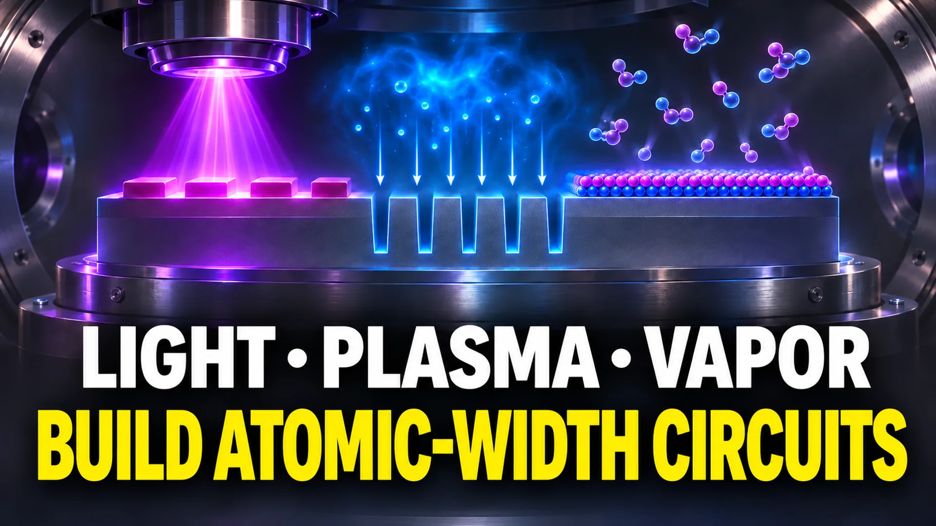
In a 2-nanometer (nm) semiconductor process, the circuit line width is roughly the width of about 40 atoms lined up side by side 1. Unlike the concept of a "thin line" that we commonly imagine, which stops at the thickness of a hair (about 80 µm, or 80,000 nm) or micrometer scales, a width of 40 atoms represents an extreme scale bordering on the atomic world. Such narrow widths are not engraved by a single precision machine in one go. Instead, they are created through the alternating operation of three types of machines—drawing the blueprint with light, carving away material with ionized gas, and depositing material layer by atomic layer with reactive vapor—dozens to over a hundred times 2.
Understanding the full skeleton of chip manufacturing makes this easier to grasp. A semiconductor is a material with properties intermediate between a conductor and an insulator, and it can control electrical flow via its bandgap (the energy gap electrons must jump to reach the conduction band; in semiconductors, this is approximately 1–3 eV) 2. The process of doping—mixing in phosphorus or boron to alter the conductivity of specific regions—and then laying down metal wiring to form transistors is repeated on the wafer. These processing steps are repeated dozens to over a hundred times 2. In this process, key roles are divided among lithography scanners, etchers, and deposition tools.
Lithography Scanner: Drawing the Blueprint with 13.5 nm Light
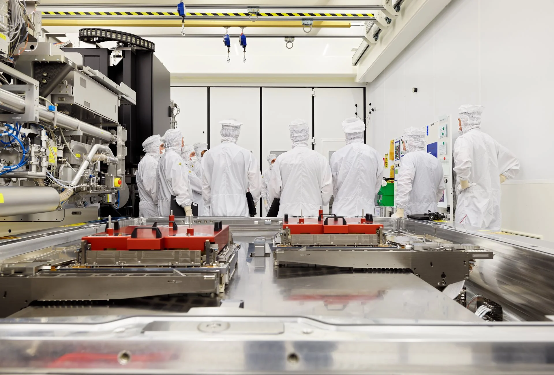
The primary step of transferring circuits onto a wafer is called lithography (photolithography). This process consists of three main stages: photoresist application → light exposure (lithography) → development 2. Photoresist is a material whose chemical properties change when exposed to light. After exposure, applying a developer washes away only the areas exposed to light (or the areas not exposed, depending on the resist type), leaving behind ridges or grooves in the pattern of the designed circuit on the wafer 2. This is akin to transferring a pattern onto a surface, much like developing a photograph.
The problem the equipment must solve here is the "diffraction" of light. When shrinking an image with lenses, longer wavelengths of light cause fine patterns to blur. Therefore, to draw finer lines, the wavelength must be reduced 3. The semiconductor industry's trend of continuously shortening wavelengths according to this principle is well-documented. Starting from visible light, DUV (deep ultraviolet) was the primary tool for some time at 193 nm, followed by EUV (extreme ultraviolet) at 13.5 nm (photon energy 92 eV) 3. EUV lithography systems, which reduce the wavelength by 1/14, were developed as tools to handle fine line widths below 22 nm and further around 10 nm 3.
As wavelengths become shorter, mirrors must replace glass lenses, and a vacuum environment becomes necessary. The transition to EUV introduced changes impossible with conventional optical systems, described in technical articles as requiring "everything to operate in a vacuum and demanding reflective optics" 3. Additionally, as circuit widths shrink, the chemical composition of the photoresist becomes a critical variable. In a 2015 study published in Scientific Reports, researchers compared 13.5 nm and 6.5 nm (BEUV) using interference lithography. They found that a hafnium-based inorganic photoresist (Inpria IB) achieved an 18 nm half-pitch (half the period of the line-and-space pattern) at both wavelengths. In contrast, the organic chemically amplified resist (CAR) saw its minimum achievable half-pitch nearly double under BEUV compared to EUV (18 nm) 3. This indicates that as light energy increases, the variance in outcomes depends significantly on how the molecular backbone of the photoresist responds to it. This demonstrates that lithography scanners are not simply tools that emit "fine light"; the chemistry of the photoresist reacting to that light is also part of the design scope.
Etcher: Erasing Outside the Blueprint with Plasma Ions
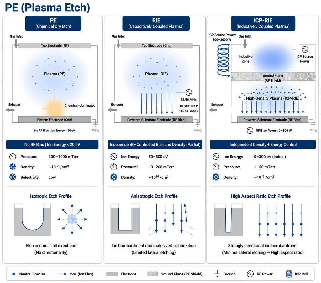
If lithography is the stage that leaves only the blueprint, etching is the stage that actually carves the circuit shape. Etching is the process of removing unnecessary parts after exposure using chemical solutions or plasma, leaving behind only structures in the shape of the circuit 2. In modern processes handling fine patterns, dry etching is essential. Wet (chemical) etching is fast but tends to etch uniformly in all directions, causing narrow widths to blur. Dry etching, however, can carve vertically by firing ions directionally 4.
Plasma, the key medium for dry etching, is an ionized gas created by applying energy to a gas, stripping electrons from atomic or molecular bonds. It is an electrically conductive medium containing a mix of free electrons, ions, and neutral particles 5. When ions are accelerated by an electric field to collide vertically with the wafer surface, physical and chemical reactions occur. This enables anisotropic etching, where only the areas exposed beneath the photoresist are precisely carved away 4. Plasma is generated through methods such as inductively coupled plasma (ICP, generating an electromagnetic field with a coil), capacitively coupled plasma (CCP, using parallel electrodes), and electron cyclotron resonance (ECR, increasing density with a magnetic field). The energy sources used are categorized into RF (radio frequency), microwave, and direct current. RF allows flexible control of ion energy, making it suitable for etching. Microwave is used for high-density plasma processes requiring precision, and direct current is primarily used for physical deposition methods like sputtering 5.
Because variables such as ion energy, gas flow rates, and chamber pressure are interconnected and influence each other, the difficulty of control increases as etchers advance to finer processes. The etcher itself should not be understood as an independent solution, but as a component responsible for the precision of one step out of dozens.
ALD Deposition Tool: A Stamp That Adds Just One Atomic Layer at a Time
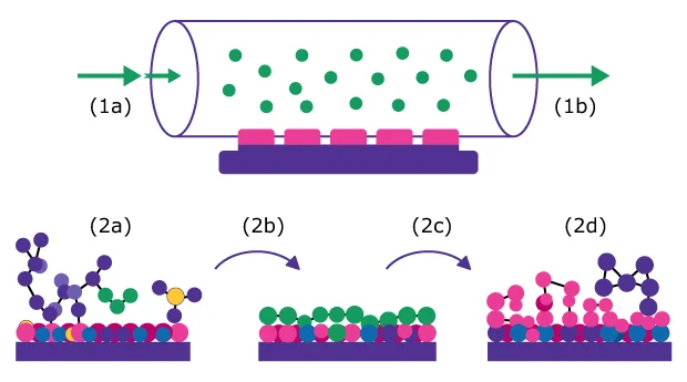
Deposition is the stage where new films are laid onto the areas carved out. For latest-generation structures where thickness must be controlled at the atomic level, atomic layer deposition (ALD) serves as the key tool. ALD is a technology capable of uniformly applying ultra-thin films required for nanoscale devices, such as the gate oxide layer of a MOSFET, even on complex 3D structures. It is essential for highly integrated devices 5.
The reason ALD can build films layer by atomic layer lies in a chemical property known as a "self-limiting reaction." The Merck Millipore CVD/ALD precursor guide describes the cycle in four steps 6.
- ① When the first precursor (source molecule) is introduced into the chamber, the molecules adsorb onto active sites on the substrate surface.
- ② Once all the empty sites on the surface are filled, no further adsorption occurs (saturation, self-limiting).
- ③ The remaining residual gas is pushed out via purge.
- ④ When the second precursor is introduced, it reacts with the first layer pre-adsorbed on the surface to complete a compound one atomic layer thick 6.
The core of the process is step ②. Because the reaction physically stops when the surface is saturated, "over-deposition"—where the film becomes thicker or thinner than expected—does not occur even if the same cycle is repeated 100 times. The principle is similar to a stamp that stops leaving a mark once the ink pad is full. To achieve a specific thickness, one only needs to adjust the number of cycles. During this process, factors such as precursor saturation characteristics, purge efficiency, and process windows must be precisely evaluated. Unlike CVD, precise sequential reaction control is decisive 6.
There are cases demonstrating why this level of precision matters at 2 nm era scales. A joint research team from Kurt J. Lesker Company, Penn State University, MIT, and the U.S. Army Research Laboratory published a study in Nature Communications Engineering specifying that the line width in a 2 nm process is at the level of about 40 atoms. They performed plasma-enhanced ALD (PEALD) under ultra-high purity conditions to create aluminum scandium nitride (AlScN) thin films 1. By using alternative precursors with little to no oxygen and alternating AlN and ScN sub-cycles with plasma treatments inserted between them—a technique called "super cycling"—they repeated the process thousands of times to stack defect-free films with angstrom-level precision 1. As a result, the thin films with reduced oxygen and carbon contamination exhibited sharper hysteresis loops and higher remnant polarization than films produced by conventional PVD (physical vapor deposition) methods 1.
Why Three Machines Operate Alternately on a Single Wafer
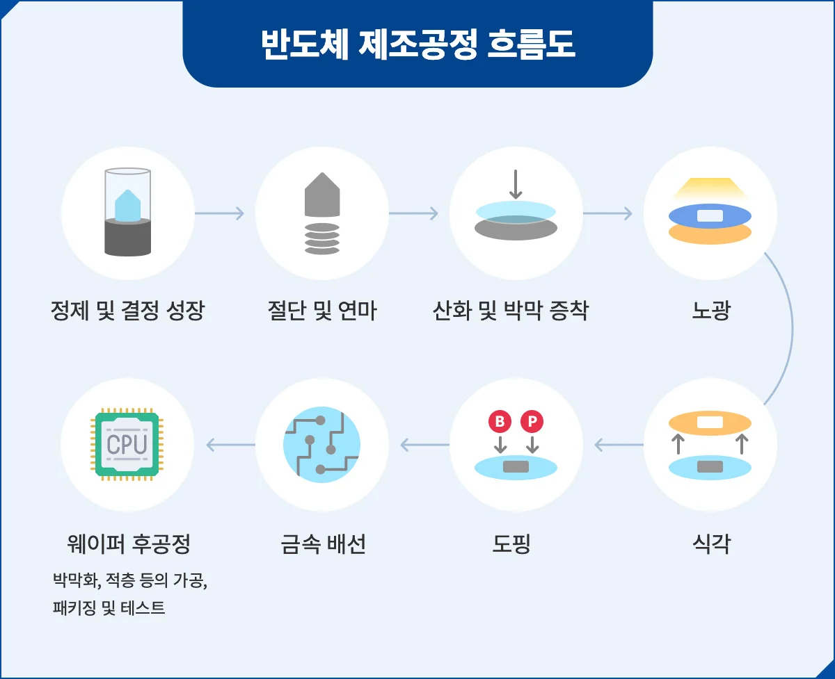
When viewed individually, each of the three machines involves complex principles. However, a single chip is manufactured by these machines operating alternately on one wafer. The steps of oxidation/thin film deposition, lithography, etching, doping, and metal wiring are repeated dozens to over a hundred times because sequences of operations like deposition, lithography, and etching do not end after a single pass 2. Each step must be performed with nanoscale precision. If any single step goes awry, the switching function of the transistors or signal transmission via metal wiring will fail to operate normally across the entire circuit network 2.
Semiconductor manufacturing sounds abstract if described only as the "repetitive operation of precise machines." However, the moment one understands the three specific physical and chemical principles—"13.5 nm light," "ionized gas accelerated by an electric field," and "self-limiting reactions that stop when the surface is filled"—the number representing a 40-atom width ceases to be a magical realm and becomes a scale that tools actually handle. A circuit is not carved by a single machine in one operation. It is the result of three machines, each ensuring precision through different principles, piecing it together dozens of times 2356.
References
- Atomic Layer Deposition of High Purity AlScN Thin Films Achieved Through Ultrahigh Purity Conditions - Semiconductor Digest · semiconductor-digest.com↩
- 반도체 제조 공정과 원리를 완벽 해설 | SEKISUI CHEMICAL – 전자재료|기술칼럼|세키스이화학공업 주식회사 |고기능 플라스틱 컴퍼니 · sekisuichemical-hppc.com↩
- Beyond EUV lithography: a comparative study of efficient photoresists' performance - Scientific Reports · nature.com↩
- 반도체 8대 공정 한 눈에 보기 - 전체 틀 쉽게 잡기 · m.blog.naver.com↩
- The Role of Plasma Technology and Deposition Techniques in Semiconductor Manufacturing | RFHIC · rfhic.com↩
- From Molecule to Thin Film: A Guide to CVD and ALD Precursor Selection · merckmillipore.com↩