As the competition in semiconductor advanced-node fabrication evolves beyond the 3-nanometer generation to the 2-nanometer node, the importance of process variables defining each individual transistor on a chip is becoming paramount. One factor exerting a decisive influence in this precise operation is 'Ultrapure Water.' With ion content approaching virtually 0%, ultrapure water is an indispensable material in semiconductor cleaning processes, and the core technology used to produce this water is 'ion exchange resin.'
Keeping pace with these ultra-fine process trends, Samyang Corporation unveiled the technical specifications and 2nm process response strategy for its ion exchange resin product line for ultrapure water production, 'TRILITE.' This unveiling extends beyond mere product promotion, drawing attention for its significance in localizing semiconductor materials and securing competitiveness within the global supply chain.
Technical Requirements of Ultrapure Water Defining Ultra-Fine Processes
As semiconductor processes shrink, the impact of trace impurities in water on chip yield and reliability becomes critical. In ultra-fine processes such as 2nm, management standards for specific impurities like boron become extremely stringent. Since boron is used as a dopant and can directly affect semiconductor performance, it requires precise control to be maintained at levels below 1ppt (parts per trillion) 1, 2.
The process for manufacturing such ultrapure water is broadly divided into pretreatment, pure water manufacturing, and ultrapure water manufacturing stages. In the final stage, the polishing system, optimized ion exchange resins are used according to the required purity grade, becoming a key variable determining the quality of the semiconductor process 2.
![Image: High-purity semiconductor manufacturing facility cleanroom with water purification piping system]
Technical Specifications and Differentiation of Samyang Corporation’s 'TRILITE' Product Line
Samyang Corporation’s 'TRILITE' ion exchange resin for ultrapure water is a product line optimized for ultrapure water manufacturing processes in semiconductors and displays. This product line features high physical uniformity with a uniformity coefficient of 1.1 or lower, and guarantees ion conversion rates of 99.9% or higher for H⁺ and 97.0% or higher for OH⁻ 1, 2. Thanks to these characteristics, it maintains high operating exchange capacity even at fast flow rates, enabling efficient ultrapure water production 2.
The lineup is segmented according to product usage and required purity grades. The general electrical and electronic grade 'UPRM100U' applies a resistivity standard of 17.0 MΩ·cm or higher, while the display and semiconductor grade 'UPRM300U' applies standards of 18.2 MΩ·cm or higher for resistivity and less than 1 ppb for TOC (Total Organic Carbon). The top-tier semiconductor grade 'UPRM400U' strictly manages metal impurities in addition to these criteria, enabling ultra-fine control of ions and organics 2.
In particular, 'CLR-B3UP' is drawing attention as a key card for responding to the 2nm process. This is a resin dedicated to boron removal, featuring performance with a total exchange capacity of 0.9 eq/L or higher and a boron exchange capacity of 0.4 eq/L or higher. This dedicated resin is designed to effectively control boron impurities, thereby contributing to extending the lifespan of the polishing system and improving process yield 2.
![Image: Close-up of high-performance ion exchange resin beads with semiconductor wafer background]
Foundation of 'Uniform Particle Size Ion Exchange Resin' Technology Built Over 50 Years
Samyang Corporation’s technology in ultrapure water materials is the result of a long history that began with being the first in South Korea to produce ion exchange resins in 1976. The company successfully developed ion exchange resins for ultrapure water in 2011, laying the foundation for localizing domestic materials, which has recently led to the commercialization of products for semiconductors 1.
The physical basis enabling this technological progress is the ion exchange resin plant located in Gunsan with an annual production capacity of 20,000 tons. Boasting the largest scale in Asia, this facility is core infrastructure capable of mass-producing 'uniform particle size' ion exchange resins, a high-difficulty process. It is known that only four companies worldwide are capable of producing uniform particle size products in the global ion exchange resin market 1.
Market research indicates that the global ion exchange resin market is valued at approximately 2 trillion won, showing an annual average growth rate of 4–5%. In particular, the domestic ultrapure water market is projected to expand to approximately 1.5 trillion won in 2026, suggesting an opportunity to replace the market, which has traditionally relied heavily on U.S. and Japanese firms, with domestic technology 1.
![Image: Large-scale industrial resin production plant exterior in Gunsan]
Collaborative Ecosystem and Strategic Moves for Technology Localization
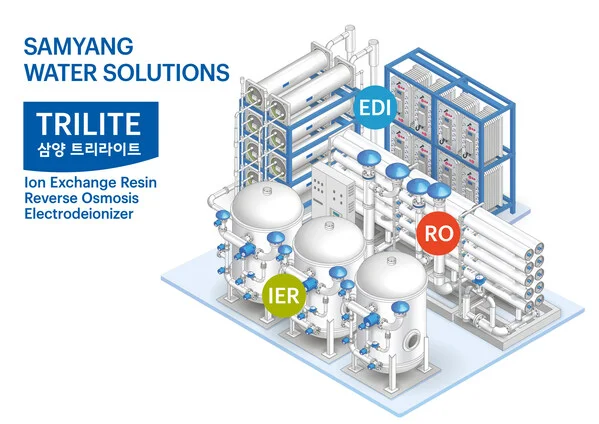
Samyang Corporation has signed a Memorandum of Understanding (MOU) with Hansung Cleantec and established a cooperative system to localize ultrapure water production technology. This structure involves Samyang Corporation supplying the ion exchange resin 'TRILITE,' while Hansung Cleantec handles equipment design and construction 1.
The combination of a materials company and an equipment company is interpreted as a strategy accelerating the 'localization of the entire ultrapure water production system' operating in the field, going beyond the standalone performance of the material. Amid the global trends of the circular economy and the localization of materials, parts, and equipment, this is part of the effort by Korean companies to secure control over core technologies, moving beyond simple manufacturing 1.
Ultimately, Samyang Corporation’s unveiling of its ultrapure water materials presents a material solution to the technical requirements of the semiconductor 2nm process, while also serving as a significant milestone that elevates the supply chain stability and technological self-reliance of the domestic semiconductor industry.
References
- 세계 순환경제 영향력 확대하는 韓기업들 < 중공업/화학/에너지 < 산업... · ezyeconomy.com↩
- 초순수 이온교환수지 | 반도체 초순수 | 삼양사 TRILITE · samyangtrilite.co.kr↩